FinFET vs Gate-All-Around: Why Did GAA Take 34 Years?
How transistors moved from planar to FinFET to gate-all-around, and why GAA, demonstrated in 1988, only reached volume production at Samsung in 2022.

What is the difference between FinFET and gate-all-around transistors?
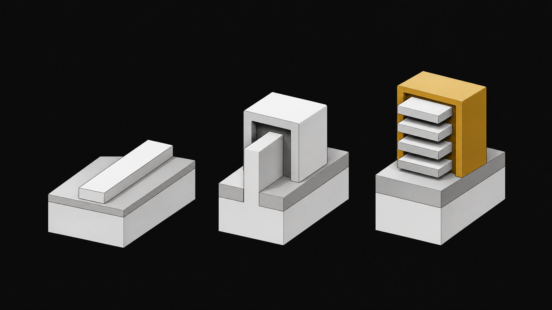
A FinFET shapes the transistor channel into a thin vertical fin, and the gate wraps the fin on three sides. A gate-all-around (GAA) transistor slices the channel into thin horizontal ribbons, and the gate surrounds each ribbon completely, including the bottom. More contact means tighter control over the channel and less leakage when the switch is off. GAA was demonstrated in 1988 but did not reach volume production until Samsung's 2022 chips.
TL;DR
- Transistor history is a progression from two dimensions into three, and each step gives the gate more contact with the channel.
- Planar gates touch the channel from the top, FinFETs from three sides, and GAA from all sides.
- GAA needs a temporary placeholder material between the ribbons, because the real gate materials would not survive wafer processing at around 1,000° C.
- GAA also requires high-k insulators and metal gates to be deposited around every suspended ribbon, which called for new tools, gases and hardware.
- FinFET was demonstrated in 1989 and shipped at Intel in 2011, while GAA, shown a year earlier, shipped at Samsung in 2022.
- The delay was partly a matter of timing: nobody tackled GAA until easier performance gains ran out.
How does a transistor work?
A transistor is a switch. When it is on, current flows between two ends called the source and the drain. A gate sits above the silicon between them. A positive voltage on the gate pulls negatively charged electrons up toward it. A thin insulating layer stops them from reaching the gate, so they collect just beneath it and form a conducting path from source to drain. That path is the channel.
Remove the voltage and the electrons disperse. The channel disappears and the switch turns off.
Why did transistor designs have to change?
Shrinking caused the problem. As transistors got smaller, the source and drain moved so close together that current could leak through the channel even when the switch was supposed to be off.
The fix was to give the gate a tighter grip on the channel by touching it from more sides. Every major redesign since the planar MOS transistor of 1960 follows that logic.
How do planar, FinFET and GAA transistors compare?
| Design | Channel shape | Gate contact |
|---|---|---|
| Planar | Flat layer in the silicon | Top only |
| FinFET | Thin vertical fin | Three sides (top and both sides) |
| Gate-all-around | Stacked thin ribbons | All sides, including the bottom |
The FinFET squeezes the channel into a fin, and the gate drapes over it like a saddle. GAA goes further. It slices the channel into ribbons and wraps the gate around each one. Chris, the engineer interviewed in the source clip, called GAA "really the ultimate transistor."
How is a gate-all-around transistor built?
The ribbons have to float, and that creates a manufacturing puzzle. The process looks roughly like this:
- Build a stack that sandwiches the silicon ribbons between alternating layers of a temporary placeholder material. The placeholder holds the space where the gate will go.
- Run the high-temperature processing steps, which bake the wafer at around 1,000° C. The real gate materials could not survive this, which is why a placeholder is used.
- Etch away the placeholder, leaving the ribbons suspended.
- Coat every ribbon with a thin layer of a high-k insulator. This lets the gate pull more strongly on the channel.
- Deposit the metal of the gate on top of the high-k material, filling the gaps around each ribbon.
Step 4 and 5 are harder than they sound. In a FinFET, the high-k metal gate goes onto an exposed fin. In GAA, it has to reach into narrow gaps around ribbons, so engineers had to work out how to put high-k metal gate in with gate-all-around.
Why did GAA take 34 years to reach production?
The dates are 1988 for the GAA demonstration and 2022 for Samsung's first production chips. FinFET went from a 1989 lab demo to Intel volume production in 2011. The two ideas appeared around the same time but shipped a decade apart.
According to the engineer in the source, the reasons were practical:
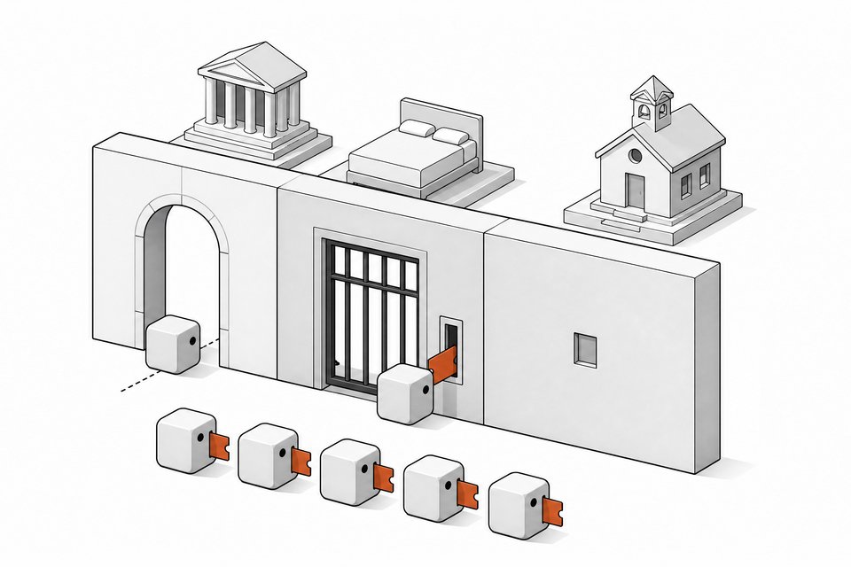
- Known problems, no urgency. In the 1990s the industry already knew GAA would be hard to manufacture at volume. Other options were available that improved performance with less pain, including strained silicon, high-k metal gate and FinFETs. His summary: "you don't want to tackle something before you have to."
- Materials. Sometimes a new design needs a new material.
- Tooling. Sometimes it needs a different tool. That means asking tool vendors for a machine that does a specific job, a gas that deposits a particular material, or a heating chuck with certain characteristics. Each of those takes invention and time.
- Iteration. Teams build a GAA transistor, see that it did not work, work out what was wrong with their hypothesis and try again.
Once the earlier techniques were used up, the industry needed further gains, and the hard problems of GAA became worth solving.
How did chip R&D change after the Dennard scaling era?
In the 1980s and 1990s, progress was driven by Dennard scaling and lithography. Make transistors smaller and they got faster and more reliable, on a predictable cadence. The process flow stayed largely the same. As the engineer put it, you just "scale it, scale it, scale it."
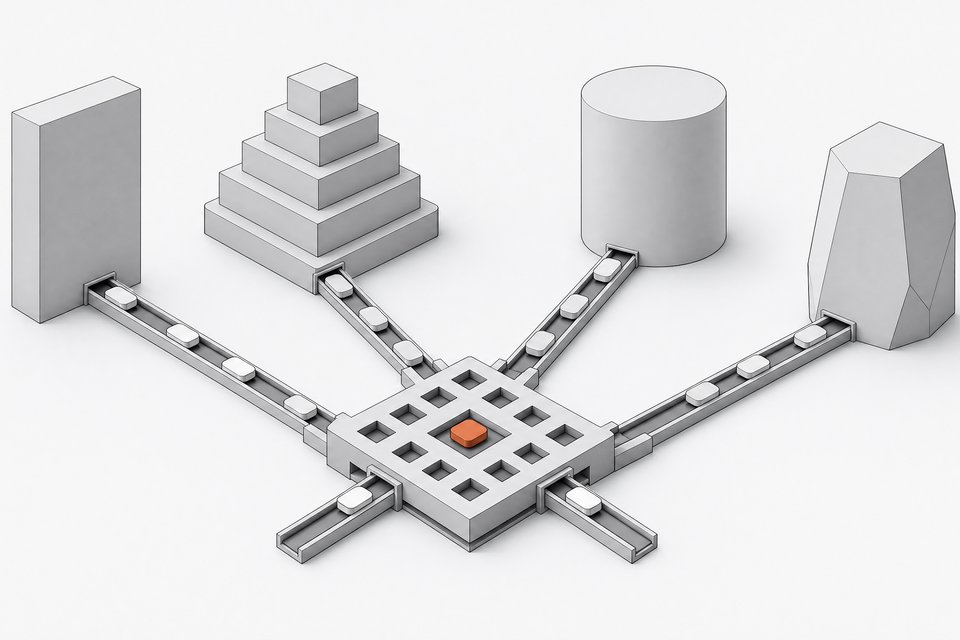
In the 2000s that stopped being enough. Each technology node needed its own answer for more scaling and more performance. That pressure produced:
- strained silicon
- high-k metal gates
- FinFETs
- gate-all-around
- backside power
He described this as a "golden age of innovation." Ideas that would have been rejected in the 1990s because they disrupted the process flow became standard. He estimated that the number of materials used has probably gone up 10x since the 1990s, and he pointed to atomic layer deposition, which controls material growth atom by atom. The attitude shifted from trying not to change anything to tearing things up when a new idea needs it.
Is GAA the end of transistor evolution?
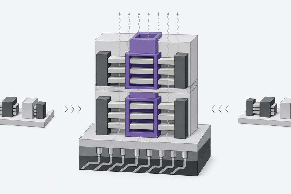
Not according to the source. Backside power is listed alongside GAA as another product of the same pressure to find new performance gains at each node. The source does not go into backside power in detail, so it is best read as the next item in the same trend rather than a finished story. The pattern holds: when simple shrinking stops delivering, the industry reaches for the next idea it has been holding in reserve. One candidate for that reserve is the CFET, which stacks N-type and P-type transistors.
Frequently Asked Questions
What does gate-all-around mean?
It means the gate surrounds the channel completely. In GAA transistors, the channel is cut into thin ribbons and the gate wraps around each ribbon on every side, including the bottom.
When did FinFET and GAA first reach production?
FinFET reached volume production at Intel in 2011, after a 1989 lab demonstration. GAA was demonstrated in 1988, and Samsung began producing GAA chips in 2022.
Why is a placeholder material used in GAA manufacturing?
The real gate materials would not survive processing that includes baking the wafer at around 1,000° C. A placeholder holds the space during those steps, then gets etched away to leave suspended ribbons that are filled with high-k insulator and metal gate.
What is a high-k material?
It is a special insulator coated around the channel. Its purpose is to let the gate pull more strongly on the channel.
Why did leakage become a problem?
As transistors shrank, the source and drain moved so close together that current could flow through the channel even when the switch was meant to be off. More gate contact on the channel is the main answer to that.
How we source, write, and correct our articles. Editorial standards