Why Does Intel 14A Use High-NA EUV When TSMC Doesn't?
Backside power relaxes front-side pitch, so Intel can print 14A layers in one high-NA pass while TSMC sticks to double-patterned EUV. Plus Intel's PDK lessons.

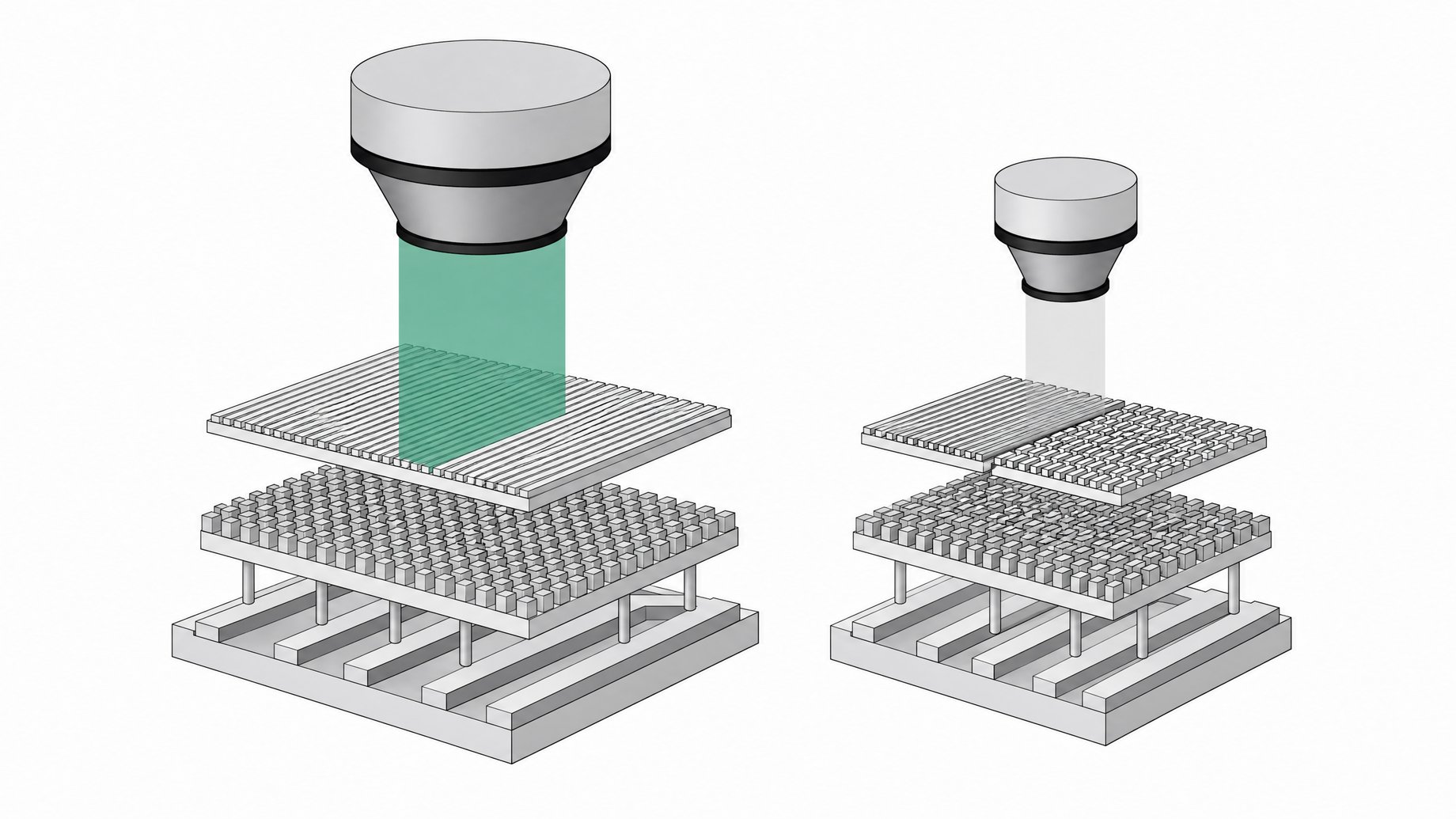
Why does high-NA EUV make sense for Intel 14A but not for TSMC?
Intel uses backside power, which moves power lines under the transistors and loosens the wire pitch on the front side. That looser pitch can be printed in a single high-NA EUV pass. TSMC, according to Intel's account, has no backside power on the comparable node, so it must run tighter front-side pitches. Those still need double-patterned standard EUV, so the pricier high-NA tool doesn't help it yet.
TL;DR
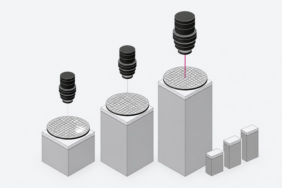
- Numerical aperture is the key spec: standard EUV tools have an NA of 0.33, and high-NA tools reach 0.55, which prints features about 1.7 times smaller in one pass.
- Smaller single-pass features mean fewer multi-patterning steps, which saves tool time and cuts defect risk.
- High-NA machines cost about twice the roughly $200 million of a standard EUV tool, so the savings must outweigh that premium.
- Intel's backside power relaxes front-side pitch enough that one high-NA pass can print layers that would otherwise need several.
- Intel has left high-NA on 14A as an option in the PDK, decided customer by customer.
- Intel's 18A began without a PDK, and the company says 14A will have a mature PDK from the start.
What does numerical aperture mean in EUV lithography?
Numerical aperture (NA) measures how wide a cone of light a lithography machine's mirrors can focus onto the wafer. A wider cone focuses to a smaller spot, and a smaller spot carves smaller features.
Today's standard EUV machines have an NA of 0.33. High-NA machines widen that to 0.55. Both use the same extreme ultraviolet light. The change is in the optics, not the light source.
| Standard EUV | High-NA EUV | |
|---|---|---|
| Numerical aperture | 0.33 | 0.55 |
| Relative single-pass feature size | Baseline | About 1.7x smaller |
| Approximate tool cost | Around $200 million | About twice that |
Why does multi-patterning matter so much?
When the features you want are smaller than the machine can print in one shot, chipmakers split the pattern across several passes. Each pass prints a different subset of features. The most tightly packed layers can need two, three, or even four passes.
That has two costs:
- Each pass occupies a machine that costs around $200 million, so every extra pass eats expensive tool time.
- Each pass is another chance to introduce defects, and alignment between passes adds risk.
A high-NA tool can collapse several passes into one. The economic question is simple. Do the time saved and the defect risk avoided outweigh a machine that costs about twice as much? The answer depends on which layers you need to print and how tight they are.
How does backside power change the high-NA math?
A chip has two kinds of wiring. Power lines deliver electricity to the transistors and need to be thick. Signal lines let transistors talk to each other. They are thinner, but they need spacing so one signal doesn't interfere with its neighbor.
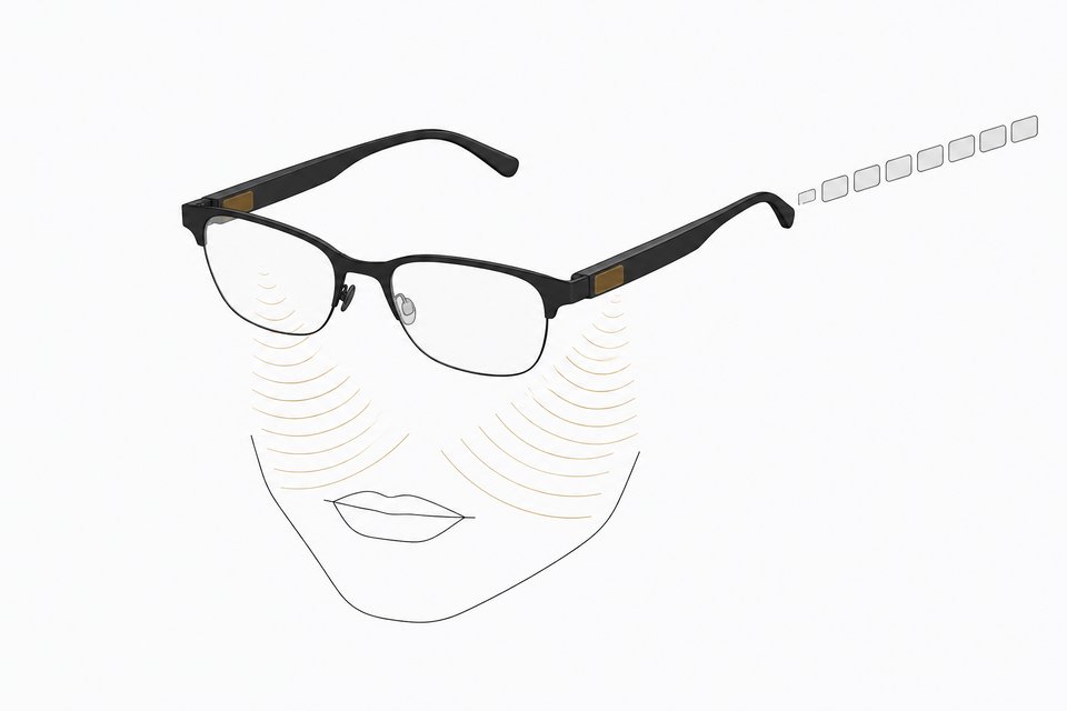
Historically, both sat together in the stack above the transistors. Intel's newest process moves the power lines beneath the transistors, to the back of the wafer. That frees room on top, so signal lines don't have to be packed as tightly.
Intel's explanation is that this is what tips the balance. Without backside power, the front-side wiring is so tight that it would need multiple passes even on a high-NA tool. With it, a single high-NA pass is enough. In the words of Intel's executive in the interview, the same tool set leads to different conclusions because the architectures differ.
Why is TSMC skipping high-NA for now?
TSMC has said high-NA doesn't make economic sense for it yet. Intel's view of why: without backside power, TSMC has to hold very tight pitches on the front side. High-NA can't print those in one pass, so TSMC falls back on double-patterned standard EUV. If you still need multiple passes, paying double for the tool buys little.
This is Intel's characterization, not TSMC's own explanation. TSMC's stated position is only that the tools aren't economical for it yet. The word "yet" matters. Pitch requirements, tool pricing, and throughput all shift over time, and the calculation can change with them.
Is high-NA locked in for Intel 14A?
No. Intel says it has left high-NA as an option on 14A. It appears in the PDK today, and Intel handles the choice as a customer-by-customer discussion. The executive described a real value proposition, but also added complexity.
That makes sense for a foundry. A customer weighing cost, schedule, and design rules may prefer one path over another, and Intel is keeping both open rather than forcing the decision.
What went wrong with Intel's 18A PDK?
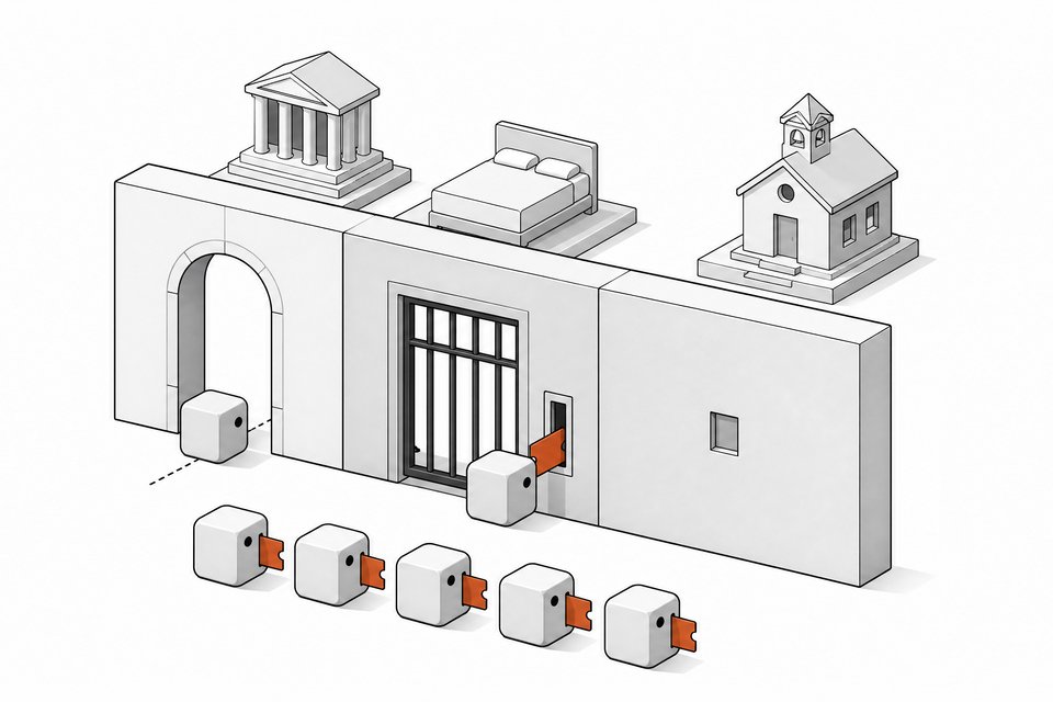
A process design kit (PDK) is the menu of what a process can build, plus the rules for building it. Outside customers design their chips against it. If the PDK is incomplete or wrong, designers hit instructions that don't work and the foundry becomes hard to use.
Public reporting described delays and problems with the 18A PDK. Intel's response was candid about the cause. For decades it was an integrated device manufacturer (IDM), meaning its fabs served its own product teams. Those teams got transistor data directly and shared it informally, with no formal PDK process. As Intel put it, 18A started out without a PDK, so the company had to build that process while customers were already giving feedback on quality, maturity, and content.
Intel says it has absorbed that feedback. Its claims for 14A:
- 14A will have high-quality PDKs from the start.
- Intel tracks maturity metrics, such as the difference between a 0.5, a 0.9, and a 1.0 PDK.
- Customer feedback keeps flowing back into PDK quality.
These are Intel's statements of intent. Customers will judge them once real 14A designs begin.
Does serving only itself explain Intel's foundry gap?
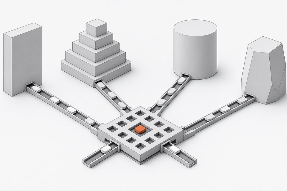
It's part of the story. Because Intel's fabs mostly made Intel's chips, the company lacked the wide customer base that TSMC enjoys. Many customers mean more wafers to learn from, more revenue to reinvest, and more pressure to meet deadlines. A foundry-grade PDK is one visible product of that pressure.
Frequently Asked Questions
What is the difference between 0.33 NA and 0.55 NA EUV?
Numerical aperture describes how wide a cone of light the optics can focus. At 0.33, standard EUV tools resolve a certain minimum feature size. At 0.55, high-NA tools print features about 1.7 times smaller in a single pass. That can replace multiple patterning steps on tightly packed layers.
Does high-NA EUV always beat double patterning?
No. High-NA tools cost about twice as much as standard EUV machines. They pay off only when they remove enough passes and defect risk to offset that price. If a layer still needs multiple passes even with high-NA, the advantage mostly disappears.
What is backside power delivery?
It is a design that places power lines beneath the transistors, on the back of the wafer, instead of in the same wiring stack as the signal lines. Power lines need to be thick, and signal lines need spacing. Separating them lets the front-side signal wiring spread out.
Will every Intel 14A customer use high-NA?
Not necessarily. Intel describes high-NA as an option in the 14A PDK, discussed with each customer. Some may take it for the value it offers, while others may avoid the added complexity.
How we source, write, and correct our articles. Editorial standards