What Is a CFET? Gate-All-Around and Chip Scaling Limits
A CFET stacks N-type and P-type transistors to save space. Learn how gate-all-around and backside power work, and why heat limits 3D chip scaling.

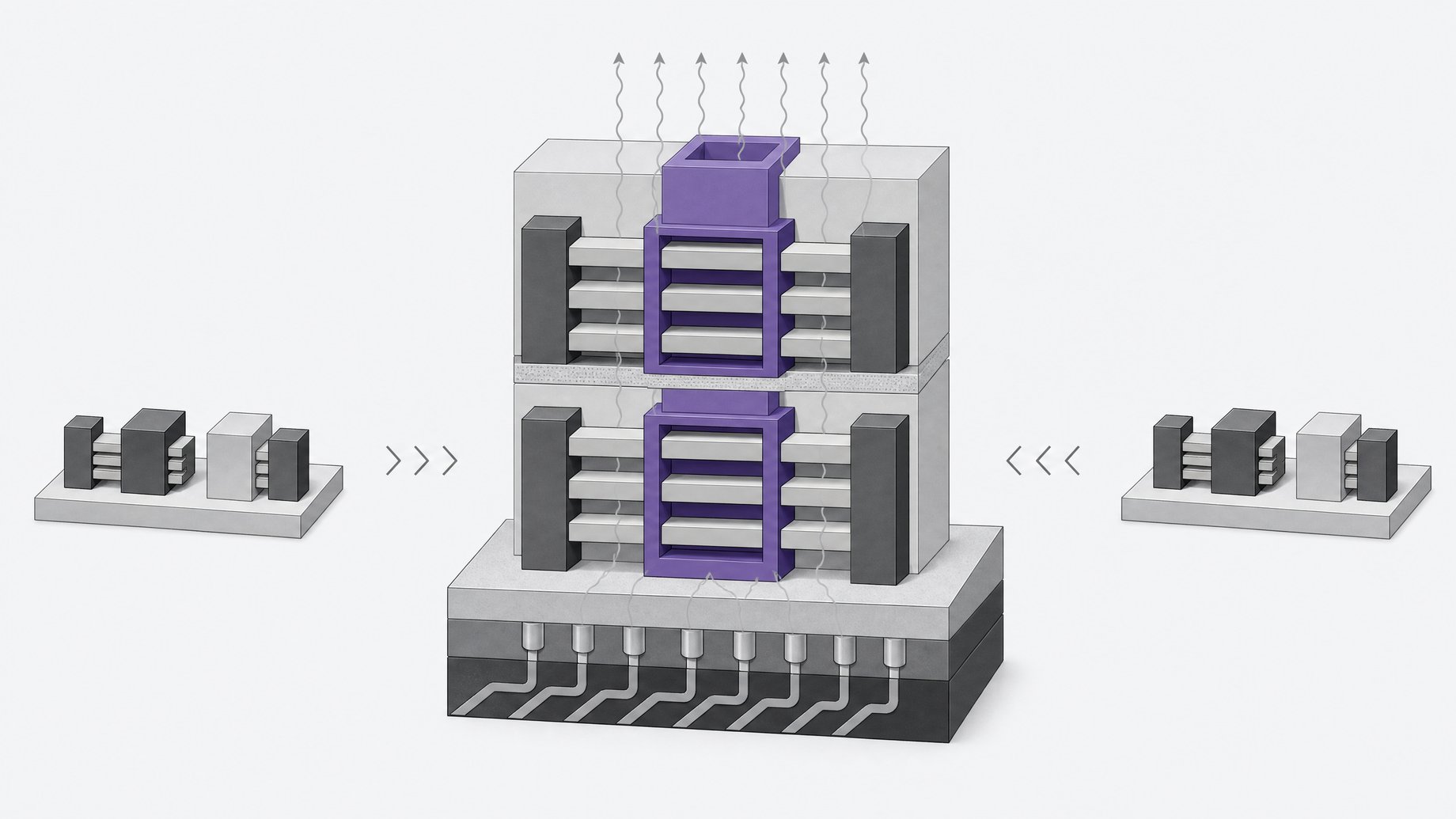
What is a CFET?
A CFET, or complementary field-effect transistor, stacks the two transistor types that make up nearly every logic circuit directly on top of each other. Chips pair N-type and P-type transistors, which work the same way with the charges reversed. Today chipmakers place them side by side. A CFET puts one above the other, which in principle fits twice as many transistors into the same area. The tradeoffs are extra manufacturing steps, higher cost, and heat with no clear way out.
TL;DR
- A CFET stacks N-type on P-type transistors instead of placing them side by side, which in principle doubles transistor density in the same footprint.
- Gate-all-around transistors and backside power change the chip from "substrate with layers on top" to a transistor embedded in interconnect, which opens the door to more 3D structures.
- Every added layer brings more process steps, more cost, and trapped heat.
- Logic burns more power than memory, so stacking logic is harder than stacking DRAM or NAND.
- Three things limit compute: switching speed, switching power, and heat removal. Thermals are the hardest of the three in 3D designs.
- Chipmakers have roughly four years of clear visibility. Beyond that, including whether copper survives at the tightest pitches, the picture gets fuzzy.
What is a gate-all-around transistor?
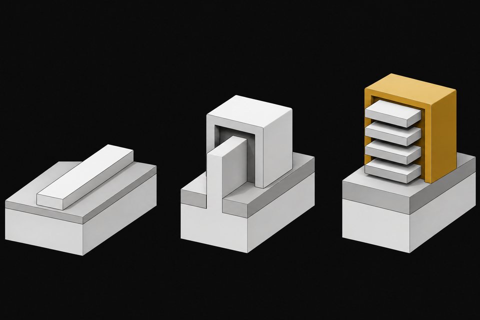
A transistor is a switch. A gate controls whether current flows through a channel. In older planar designs the gate sat on top of the channel. FinFETs raised the channel into a fin so the gate could touch it on three sides. Gate-all-around (GAA) takes the next step and wraps the gate around the channel on every side, which gives tighter control over the current.
The idea is not new. People were already discussing this kind of structure in the 1990s, and one chip-industry view is that GAA is close to the ideal transistor structure and its arrival was somewhat inevitable. The concept sat on the shelf for decades until the manufacturing caught up.
How does backside power change chip design?
Conventional chips build transistors on a silicon substrate and stack all the wiring above them. Power lines and signal lines compete for the same space. Backside power moves the power delivery to the other side of the wafer, so the front can focus on signals.
That sounds simple. It is not. It means thinning or removing the silicon substrate and building wiring on the back of the transistor layer. Even in the 1990s, the idea of stripping off the whole substrate and putting lines on the backside was considered a stretch. It is now a real part of the roadmap.
Why do GAA and backside power point toward 3D stacking?
Once you have gate-all-around transistors and backside power, the chip stops looking like a flat substrate with layers piled on top. You have a transistor suspended in interconnect, with wiring on both sides. That raises an obvious question: why not alternate transistors, interconnect, more transistors, more interconnect?
We already do a version of this by stacking discrete chips. The CFET pushes the same logic down to the transistor level. Instead of stacking finished dies, you stack the devices themselves.
Why stack N-type and P-type transistors?
Logic gates rely on pairs. The N-type device and the P-type device work together in nearly every basic circuit, which is why it is called complementary. Because they are always paired, they are a natural candidate for vertical stacking. Put one on top of the other, and in principle you fit twice as many transistors into the same area.
| Approach | Layout of N-type and P-type | Area effect |
|---|---|---|
| Today | Side by side | Baseline |
| CFET | Stacked vertically | In principle, twice the transistors in the same area |
"In principle" matters here. The density gain on paper does not account for the added process complexity, the wiring needed to reach both devices, or the thermal cost.
Why is heat the central problem?
Memory already shows that vertical stacking works. 3D NAND is built this way, and HBM stacks DRAM dies. Logic is different because it consumes more power than memory. Stack logic layers and the heat generated in the middle has a hard time getting out.
Three factors limit compute:
- Frequency. How fast the device can switch.
- Power efficiency. How much energy each switch takes.
- Thermals. How you dissipate the heat that switching creates.
None of these is a new problem. Articles on all three go back 20 years. But 3D devices make the thermal piece sharper, because every layer you add sits farther from wherever the heat can leave.
One view from inside the industry is that solving this needs system-level analysis and simulation tools, and that those tools are still in their infancy because people have only recently started looking at the problem this way. Thermals will remain a limiter, but they are the kind of problem engineers can work on.
Will copper be replaced?
Copper is the best wiring material for most jobs, and for larger lines it is likely to stay. The expectation is different for the tightest pitches. As wires shrink, another material will probably replace copper there. So the likely outcome is a mix: copper for coarser lines, something else where the wiring is finest.
Is 3D DRAM coming?
NAND already uses extreme 3D structures. DRAM makers talk about doing the same, and the argument is that DRAM will inevitably go there too. A common objection is that it cannot be done in the next five years. That objection changes if you stretch the timeline. Ask about 10 years, 20 years, or 2045, and exotic structures start to look plausible.
How far ahead can chipmakers actually see?
About four years. Engineers can say what they expect to be able to build over that window. When they get there, they usually see another four years of workable steps. Beyond roughly 10 years, it becomes hard to say what the technology will look like.
This matters for reading roadmaps. Near-term items like gate-all-around and backside power are grounded in work already underway. Longer-term items like CFETs, 3D DRAM, or non-copper wiring are directions with real logic behind them, not guarantees. The tech tree may also branch in ways nobody currently expects, the way gate-all-around itself spent decades as an idea before becoming a product.
What does this mean for people building with AI?
AI workloads are limited by the same three factors: speed, power, and heat. Denser transistors help only if the power and thermal budget can handle them. The memory side already shows the shape of the tradeoff, since stacked DRAM works partly because memory draws less power than logic. Watch how thermal solutions develop alongside new transistor structures, because they may decide how much of the density gain turns into usable performance.
Frequently Asked Questions
What does CFET stand for?
CFET stands for complementary field-effect transistor. "Complementary" refers to the pairing of N-type and P-type transistors, which together form most logic circuits. In a CFET, the two are stacked vertically rather than placed side by side.
Is a CFET the same as gate-all-around?
No. Gate-all-around describes how a single transistor's gate wraps around its channel. A CFET describes how N-type and P-type transistors are arranged relative to each other. The two ideas can work together, since stacked devices need a well-controlled transistor structure.
Why can't logic be stacked as easily as memory?
Logic consumes more power than memory, so it produces more heat. In a stack, heat from the inner layers has limited paths to escape. Memory stacks such as HBM and 3D NAND work in part because memory generates less heat per layer.
Will chips stop using copper?
Probably not entirely. Copper remains the best choice for larger wires. For the very tightest pitches, though, replacing copper with another material looks inevitable according to one industry view, so future chips may use more than one wiring material.
How far ahead do chipmakers plan?
They have good visibility about four years out. After that, they expect to find workable steps for another four years at a time, but predictions beyond about 10 years are uncertain.
How we source, write, and correct our articles. Editorial standards